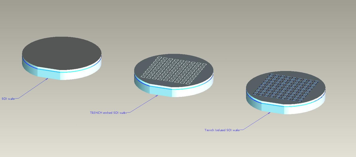
IceMOS Technology presents its dielectric isolation technology – delivering high voltage isolation between components on the same chip. Isolation is achieved using thick film SOI technology combined with state of the art high aspect ratio deep trench etching and oxide/poly refill. This technology is available on all wafer sizes from 100mm to 150mm and silicon device layers from 1.5um to 100um.
Our Trench SOI wafers are used in the following applications:
- MEMS devices
- Solid State Relay photovoltaic generators
- Photovoltaic cells and Optoelectronic devices/ICs
- High Voltage analog ICs for telecommunications
- High performance bipolar circuits
- Smart Power ICs
- Integrated Sensors
Our process engineers will work closely with your design group to realize the full potential for your processes.