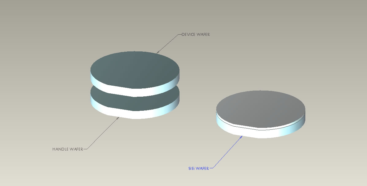
For semiconductor device manufacturers, the IceMOS SiSi bonded wafer offers a cost effective alternative to thick epitaxial layers and inverse epi that have traditionally been used for applications such as power devices and PiN diodes.
The use of direct wafer bonding technology allows silicon substrates to be produced containing multiple layers of single crystal silicon. These layers can have a resistivity range 1mΩ-cm to 10kΩ-cm., N and P-type and can include combinations of orientations – a feature not possible with conventional epitaxial wafers.
IceMOS SiSi wafers are used in the following applications:
- High voltage PIN diodes
- RF attenuators
- Photo Detectors
- X-ray detectors
- IR sensors
- HV Power Devices
- Replacement for epitaxial deposition
The IceMOS SiSi bonding process gives a high quality wafer with low leakage, low warp and a low defect density. Additionally, the thickness variation in the layers can be as little as +/-0.5um. Also, the transition between high and low dopant levels can be sharp or soft, depending on the application or customer requirement.